Introduction
PCB (Printed Circuit Board) design software is a specialized category of Electronic Design Automation (EDA) tools used to design, layout, and manufacture circuit boards that power electronic devices. These tools help engineers convert circuit schematics into physical board layouts, ensuring proper connectivity, signal integrity, and manufacturability.
As electronics become more compact and complex, PCB design software plays a critical role in reducing design errors, accelerating development cycles, and ensuring reliable performance. From consumer electronics to industrial systems, nearly every modern device depends on well-designed PCBs.
Common real-world use cases:
- Designing multi-layer PCBs for electronic devices
- Prototyping and testing circuit layouts
- Signal integrity and power analysis
- Manufacturing-ready file generation (Gerber, BOM)
- Embedded systems and IoT hardware development
What buyers should evaluate:
- Schematic capture and layout capabilities
- Routing and auto-routing features
- Simulation and signal integrity tools
- Component libraries and part management
- Ease of use and learning curve
- Collaboration and version control
- Integration with manufacturing workflows
- Cloud vs desktop deployment
- Performance for complex boards
Best for: Electronics engineers, hardware startups, PCB designers, embedded system developers, and manufacturing teams.
Not ideal for: Non-technical users, software-only teams, or projects that don’t involve hardware or circuit design.
Key Trends in PCB Design Software
- AI-assisted PCB layout: Automation of routing and component placement using AI
- Cloud-based PCB tools: Browser-based platforms improving collaboration
- Real-time design validation: Instant error detection and rule checks
- Integration with manufacturing services: Direct PCB fabrication workflows
- Open-source ecosystem growth: Tools like KiCad gaining strong adoption
- Multi-board and system-level design: Managing complex electronic systems
- 3D visualization integration: Mechanical-electrical co-design improvements
- Subscription-based pricing: Lower upfront cost models
- Improved component libraries: Better access to verified parts
- Automation of design workflows: Reduced manual intervention
How We Selected These Tools (Methodology)
- Strong adoption across industries and engineering teams
- Comprehensive PCB design and simulation capabilities
- Reliability in handling complex, multi-layer designs
- Integration with manufacturing and CAD tools
- Availability across different deployment models
- Flexibility for beginners, SMBs, and enterprises
- Quality of documentation and community support
- Extensibility via APIs and plugins
- Vendor stability and ecosystem maturity
- Balance between usability and advanced features
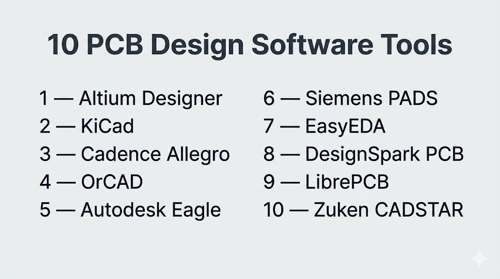
Top 10 PCB Design Software Tools
#1 — Altium Designer
Short description: A premium PCB design platform known for its unified design environment and advanced capabilities.
Key Features
- Unified schematic and PCB layout
- Advanced routing tools
- 3D PCB visualization
- Signal integrity analysis
- Component management system
- Cloud collaboration support
Pros
- Highly intuitive interface
- Strong industry adoption
Cons
- Expensive
- Windows-focused
Platforms / Deployment
Windows
Cloud / Self-hosted
Security & Compliance
Not publicly stated
Integrations & Ecosystem
Altium integrates well with modern engineering workflows and manufacturing pipelines.
- Cloud collaboration tools
- Component libraries
- APIs
- Manufacturing outputs
Support & Community
Strong documentation, training resources, and active professional community.
#2 — KiCad
Short description: A popular open-source PCB design tool used by hobbyists and professionals.
Key Features
- Schematic capture
- PCB layout editor
- SPICE simulation
- 3D visualization
- BOM and Gerber generation
- Cross-platform support
Pros
- Free and open-source
- Strong community support
Cons
- Limited enterprise features
- UI less polished
Platforms / Deployment
Windows / macOS / Linux
Self-hosted
Security & Compliance
Not publicly stated
Integrations & Ecosystem
KiCad provides a complete integrated design environment with simulation and manufacturing outputs.
- Plugins and libraries
- APIs
- Open-source tools
- Simulation engines
Support & Community
Large global community and extensive tutorials.
#3 — Cadence Allegro
Short description: High-performance PCB design tool for complex and high-speed boards.
Key Features
- Advanced routing
- Signal integrity analysis
- Constraint-driven design
- Multi-layer PCB support
- High-speed design tools
Pros
- Excellent for complex designs
- Industry-standard
Cons
- Expensive
- Steep learning curve
Platforms / Deployment
Windows / Linux
Self-hosted
Security & Compliance
Not publicly stated
Integrations & Ecosystem
- Cadence ecosystem
- Simulation tools
- APIs
- Manufacturing workflows
Support & Community
Enterprise-level support.
#4 — OrCAD
Short description: A mid-range PCB design tool offering a balance between usability and advanced features.
Key Features
- Schematic capture
- PCB layout
- Simulation tools
- Design rule checks
- Component libraries
Pros
- Balanced feature set
- Widely used
Cons
- Windows-only
- Learning curve
Platforms / Deployment
Windows
Self-hosted
Security & Compliance
Not publicly stated
Integrations & Ecosystem
- Cadence ecosystem
- APIs
- Libraries
- Simulation tools
Support & Community
Strong documentation and support.
#5 — Autodesk Eagle
Short description: A well-known PCB design tool for hobbyists and professionals.
Key Features
- Schematic and PCB design
- Auto-routing
- Scriptable workflows
- Component libraries
- Integration with Fusion ecosystem
Pros
- Easy to learn
- Good for small projects
Cons
- Limited advanced features
- Subscription model
Platforms / Deployment
Windows / macOS
Cloud / Self-hosted
Security & Compliance
Not publicly stated
Integrations & Ecosystem
- Autodesk ecosystem
- APIs
- Libraries
- CAD tools
Support & Community
Strong community and tutorials.
#6 — Siemens PADS
Short description: A scalable PCB design tool suitable for SMBs and mid-sized companies.
Key Features
- PCB layout and routing
- Signal integrity analysis
- Thermal analysis
- Design rule checks
- Component libraries
Pros
- Scalable
- Balanced cost and features
Cons
- Interface complexity
- Licensing cost
Platforms / Deployment
Windows
Self-hosted
Security & Compliance
Not publicly stated
Integrations & Ecosystem
- Siemens ecosystem
- APIs
- CAD integration
- Simulation tools
Support & Community
Strong enterprise and SMB support.
#7 — EasyEDA
Short description: A cloud-based PCB design tool designed for beginners and quick prototyping.
Key Features
- Web-based design
- Schematic capture
- PCB layout
- Simulation tools
- Manufacturing integration
Pros
- Easy to use
- No installation required
Cons
- Limited advanced capabilities
- Internet dependency
Platforms / Deployment
Web
Cloud
Security & Compliance
Not publicly stated
Integrations & Ecosystem
- Cloud tools
- Libraries
- APIs
- Manufacturing workflows
Support & Community
Growing community.
#8 — DesignSpark PCB
Short description: A free PCB design tool aimed at engineers and hobbyists.
Key Features
- Schematic capture
- PCB layout
- Design rule checks
- Component libraries
- User-friendly interface
Pros
- Free
- Easy to learn
Cons
- Limited advanced features
- Smaller ecosystem
Platforms / Deployment
Windows
Self-hosted
Security & Compliance
Not publicly stated
Integrations & Ecosystem
- Libraries
- APIs
- CAD tools
- Plugins
Support & Community
Moderate community support.
#9 — LibrePCB
Short description: A modern open-source PCB design tool focused on simplicity and usability.
Key Features
- Schematic capture
- PCB layout
- Real-time rule checking
- Component management
- Manufacturing outputs
Pros
- Open-source
- Clean interface
Cons
- Limited for complex designs
- Smaller ecosystem
Platforms / Deployment
Windows / macOS / Linux
Self-hosted
Security & Compliance
Not publicly stated
Integrations & Ecosystem
LibrePCB combines schematic, layout, and manufacturing workflows in one platform.
- Libraries
- APIs
- Open-source tools
- Export formats
Support & Community
Growing community.
#10 — Zuken CADSTAR
Short description: A professional PCB design tool used for complex and multi-layer designs.
Key Features
- Schematic and PCB design
- Auto-routing
- Signal integrity analysis
- Design rule checks
- Manufacturing outputs
Pros
- Strong professional capabilities
- Reliable performance
Cons
- Windows-only
- Learning curve
Platforms / Deployment
Windows
Self-hosted
Security & Compliance
Not publicly stated
Integrations & Ecosystem
CADSTAR supports full PCB design workflows including routing and analysis.
- CAD tools
- APIs
- Manufacturing systems
- Simulation tools
Support & Community
Enterprise-level support.
Comparison Table (Top 10)
| Tool Name | Best For | Platform(s) Supported | Deployment | Standout Feature | Public Rating |
|---|---|---|---|---|---|
| Altium Designer | Advanced PCB design | Windows | Hybrid | Unified workspace | N/A |
| KiCad | Open-source users | All major OS | Self-hosted | Free | N/A |
| Cadence Allegro | High-speed PCB | Windows, Linux | Self-hosted | Advanced routing | N/A |
| OrCAD | Mid-level design | Windows | Self-hosted | Balanced features | N/A |
| Autodesk Eagle | Hobbyists | Windows, macOS | Hybrid | Ease of use | N/A |
| Siemens PADS | SMB | Windows | Self-hosted | Scalability | N/A |
| EasyEDA | Beginners | Web | Cloud | Accessibility | N/A |
| DesignSpark PCB | Free users | Windows | Self-hosted | Simplicity | N/A |
| LibrePCB | Open-source | All major OS | Self-hosted | Modern UI | N/A |
| CADSTAR | Enterprise | Windows | Self-hosted | Professional workflows | N/A |
Evaluation & Scoring of PCB Design Software
| Tool Name | Core (25%) | Ease (15%) | Integrations (15%) | Security (10%) | Performance (10%) | Support (10%) | Value (15%) | Weighted Total |
|---|---|---|---|---|---|---|---|---|
| Altium | 10 | 8 | 9 | 7 | 9 | 9 | 6 | 8.35 |
| KiCad | 8 | 7 | 7 | 5 | 7 | 8 | 10 | 7.65 |
| Allegro | 9 | 6 | 8 | 6 | 9 | 8 | 6 | 7.75 |
| OrCAD | 8 | 7 | 7 | 6 | 8 | 8 | 7 | 7.45 |
| Eagle | 7 | 8 | 7 | 6 | 7 | 7 | 8 | 7.30 |
| PADS | 8 | 7 | 8 | 6 | 8 | 8 | 7 | 7.55 |
| EasyEDA | 6 | 9 | 6 | 5 | 6 | 7 | 9 | 7.00 |
| DesignSpark | 6 | 8 | 6 | 5 | 6 | 7 | 9 | 6.95 |
| LibrePCB | 6 | 8 | 6 | 5 | 6 | 7 | 9 | 6.95 |
| CADSTAR | 8 | 6 | 7 | 6 | 8 | 8 | 6 | 7.30 |
How to interpret scores:
- Scores are relative comparisons across tools
- Enterprise tools score high in features but lower in value
- Open-source tools offer excellent value but require effort
- Ease of use varies significantly
- Choose based on your specific workflow needs
Which PCB Design Software Tool Is Right for You?
Solo / Freelancer
- Best: KiCad, EasyEDA
- Reason: Free and easy to use
SMB
- Best: Eagle, PADS
- Reason: Balanced features and cost
Mid-Market
- Best: OrCAD, Altium
- Reason: Advanced features with scalability
Enterprise
- Best: Cadence Allegro, Altium Designer
- Reason: High-performance and reliability
Budget vs Premium
- Budget: KiCad, LibrePCB
- Premium: Altium, Cadence
Feature Depth vs Ease of Use
- Deep: Cadence, Altium
- Easy: EasyEDA, DesignSpark
Integrations & Scalability
- Strong: Siemens, Cadence
Security & Compliance Needs
- Enterprise tools preferred
Frequently Asked Questions (FAQs)
What is PCB design software?
It is software used to design and layout printed circuit boards for electronic devices.
Is PCB design difficult?
It can be complex but easier with modern tools.
What is the best free PCB software?
KiCad is widely recommended.
Can I design PCBs online?
Yes, tools like EasyEDA support browser-based design.
Do I need coding skills?
Not mandatory, but helpful for advanced workflows.
What files are generated?
Common outputs include Gerber files and BOM.
Is simulation necessary?
Yes, it helps prevent design errors.
Can beginners use PCB tools?
Yes, many tools are beginner-friendly.
How long does it take to learn?
Basic skills can be learned in weeks.
Are open-source tools reliable?
Yes, for many use cases.
Conclusion
PCB design software is essential for building modern electronic products. Whether you’re a beginner using KiCad or an enterprise team using Altium or Cadence, there are tools available for every level.